Semiconductor Defect Detection: From Manual Inspection to AI-Powered Classification
Key Takeaway
AI-powered defect classification achieves 95%+ accuracy vs 70-80% for manual inspection. Detection speed improves by several times. AI automatically identifies and correlates root causes across random, systematic, and parametric defect types.
In advanced semiconductor manufacturing, defect detection is the first line of defense in yield management. As process nodes shrink from 28 nm to 5 nm and beyond to 3 nm, a single nanometer-scale defect can kill an entire chip. The killer defect density (D0) requirement at 7 nm is below 0.1 defects/cm²; at 3 nm, this tightens further to under 0.05/cm².
The traditional manual inspection model simply cannot keep pace. An experienced defect review engineer can classify 2,000–3,000 defect images per day at best. A 12-inch fab running 50,000 wafers per month generates hundreds of thousands of defect images daily.
1. Three Technology Approaches to Defect Detection
1.1 Optical Inspection (AOI / Bright-Field / Dark-Field)
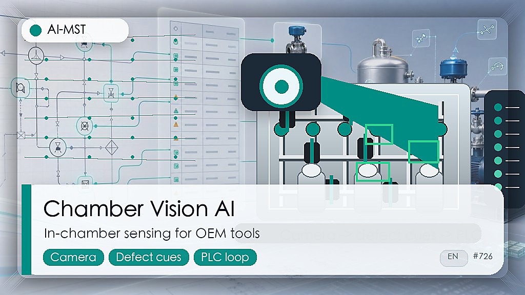
Optical inspection is the most widely deployed inline detection method in wafer fabs.
- Bright-field inspection: Best suited for patterned defects. Leading systems include the KLA 39xx series and Hitachi IS3000.
- Dark-field inspection: Extremely sensitive to particle contamination and scratches. The KLA Surfscan SP7 can detect particles down to the 12 nm range.
- Core advantage: Speed — single-wafer inspection times of 30–120 seconds make 100% inline inspection feasible.
1.2 Electron Beam Inspection (SEM / e-beam)
Resolution reaches sub-nanometer levels, far surpassing optical methods. However, throughput is the critical limitation — e-beam inspection is primarily used for sampling rather than full production screening.
1.3 Inline Process Monitoring (OES / Sensor Fusion)
Rather than detecting defects after formation, this approach monitors process parameter anomalies to predict defect occurrence in real time — flagging issues at the very moment they emerge.
2. The Core Pain Points of Defect Classification
2.1 The Dual Bottleneck of Manual Classification
Inter-reviewer consistency typically falls between 70%–85%. New engineers require 6–12 months of training before building sufficient expertise for reliable classification.
2.2 Rule Engine Maintenance Spiraling Out of Control
At the 7 nm node, defect types can number 80–120 categories. Once rule libraries expand to thousands of entries, they become virtually unmaintainable.
2.3 Data Imbalance
Common defects account for 60%–70% of all observations, while certain killer defect types may have only a few dozen samples in the training set.
3. AI-Powered Automatic Defect Classification (ADC)
3.1 CNN Image Classification
ResNet-50/101 architectures achieve top-1 accuracy of 93%–97% on defect classification tasks. EfficientNet offers a better accuracy-efficiency tradeoff for resource-constrained deployments.
3.2 Object Detection
YOLO-series models deliver exceptional speed (>100 FPS) with mAP@0.5 of 85%–92%. Faster R-CNN achieves higher precision but at roughly one-third the throughput.
3.3 Semantic Segmentation
U-Net and DeepLab-based pixel-level annotation is particularly valuable for CD-related defect analysis, where the precise shape and extent of the defect matters.
3.4 Few-Shot Learning and Transfer Learning
Transfer learning can boost accuracy on rare defect classes by 15%–25%. Few-shot learning achieves 80%+ accuracy with as few as 5–10 samples per class — critical for addressing the data imbalance challenge.
4. Where to Deploy? Edge AI Is the Only Viable Option
Production lines demand inference latency under 100 ms. Wafer defect images contain chip layout information — core intellectual property that must never leave the factory.
AI-MST’s NeuroBox E5200V is purpose-built for visual inspection scenarios at the edge. It supports local inference with mainstream architectures including ResNet, YOLO, and U-Net, with end-to-end latency under 50 ms. Deployed directly alongside inspection equipment, image data never leaves the fab.
5. From Detection to Control: Building a Quality Closed Loop
Detection alone is not enough. The real value emerges when defect insights drive process corrections in real time.
NeuroBox E5200V handles image inference on the inspection side, while NeuroBox E3200 handles data fusion and process optimization on the control side. E5200V classification results are transmitted in real time to E3200 via SECS/GEM interfaces, driving R2R and FDC systems to automatically adjust process parameters. The cycle from defect discovery to process response shrinks from days to minutes.
Related Reading
NeuroBox E3200 VM + R2R: real-time quality prediction and auto compensation on every wafer.
Learn about production AI →读完这篇,下一步可以很具体
获取一份产线 AI 评估,看看 NeuroBox E3200 / SECS/GEM 怎么接到您的设备。
把设备类型、当前数据接口、工艺目标或良率问题发给我们。工程团队会先判断适合 VM、R2R、Smart DOE、EIP 还是能源优化,再给出下一步建议。
- 适合晶圆厂、设备商、工艺/设备/自动化团队
- 可从 SECS/GEM、Modbus、PLC、CSV/历史数据开始
- 不需要先提交机密 recipe 或客户图纸
Discover how MST deploys AI across semiconductor design, manufacturing, and beyond.