Advanced Packaging Deep Dive: Equipment Challenges Behind Chiplet, CoWoS, and HBM
Key Takeaway
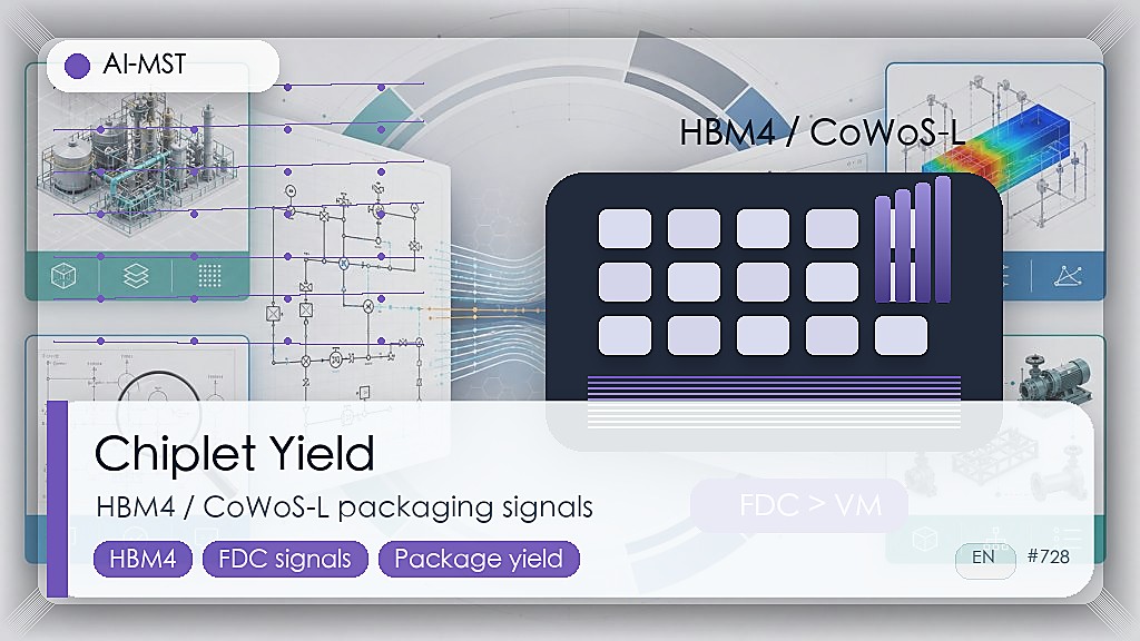
Advanced packaging (Chiplet, CoWoS, HBM) is reshaping semiconductor equipment requirements. CoWoS capacity exceeds 20% of TSMC advanced packaging. HBM stacking evolves from 8 to 12-16 layers. Equipment precision requirements reach sub-micron levels, making AI process control increasingly valuable.
Since 2025, “advanced packaging” has become the hottest keyword in semiconductors. NVIDIA, AMD, and Apple all view advanced packaging as the critical path to breaking through compute bottlenecks. TSMC’s CoWoS capacity has been oversubscribed, with lead times stretching beyond 50 weeks. SK hynix’s HBM production lines are running at full capacity, with orders booked through 2026. Behind all of this lies the convergence of three forces: the exponential demand from AI large language models for compute and bandwidth, the economic slowdown of Moore’s Law at advanced nodes, and the full establishment of chiplets as the mainstream post-Moore architecture.
Yet as the industry spotlight focuses on packaging architecture innovation, a deeper question is emerging — is the packaging equipment ready? From bonding alignment to warpage control, from yield management to process tuning, advanced packaging imposes unprecedented extreme demands on equipment capabilities. This article systematically examines the three core advanced packaging technologies, analyzes their impact on equipment requirements, and explores how AI is helping packaging equipment manufacturers and users rise to these challenges.
1. Three Core Advanced Packaging Technologies
1.1 Chiplets: Why “Disaggregate” Beats “Monolithic”
Traditional chip design pursued monolithic integration — cramming as much functionality as possible onto a single die. But as advanced node costs have skyrocketed — TSMC’s 3 nm tape-out costs now exceed $500 million — this path has become increasingly impractical. The chiplet approach embraces “heterogeneous disaggregation”: splitting a large chip into multiple functional modules (chiplets), each manufactured at its optimal process node, then interconnected through advanced packaging.
The benefits are substantial:
- Cost optimization: Compute cores at 3 nm/2 nm, I/O chiplets at mature 12 nm/7 nm — overall cost reduction of 30%–50%
- Yield improvement: Smaller chiplet die area means exponentially higher wafer yield compared to a monolithic large die
- Design flexibility: Different chiplet combinations enable product differentiation within a single family, dramatically shortening development cycles
AMD’s EPYC processor family is the chiplet benchmark: the fourth-generation EPYC (Genoa) combines up to 12 CCD chiplets at 5 nm with a single 6 nm IOD, steadily gaining server market share from Intel. Intel’s Ponte Vecchio GPU integrates over 40 chiplets across different process nodes in a single package. The UCIe (Universal Chiplet Interconnect Express) standard, jointly driven by Intel, AMD, TSMC, and Samsung since its 2023 launch, aims to establish an open chiplet interconnect ecosystem. UCIe 1.1 already supports die-to-die interconnect bandwidth density exceeding 1,300 Gbps per millimeter.
1.2 CoWoS: The Packaging Platform for AI Chips
If chiplets solve the “disaggregation” problem, CoWoS (Chip on Wafer on Substrate) solves the “reassembly” problem. Developed by TSMC, this 2.5D packaging platform introduces a silicon interposer between the chips and the organic substrate, leveraging silicon’s ultra-high routing density to interconnect multiple dies at high speed.
CoWoS advantages include:
- Ultra-high interconnect density: Silicon interposer routing pitch as fine as 0.4 µm, far superior to organic substrate’s 10–20 µm
- Ultra-high bandwidth: Chip-to-chip communication bandwidth in the TB/s range, meeting AI accelerators’ extreme data throughput demands
- Signal integrity: The interposer’s low dielectric constant and short interconnect lengths ensure high-frequency signal quality
NVIDIA’s H100 GPU uses CoWoS-S packaging, placing the GPU die alongside six HBM3 stacks on a silicon interposer of approximately 2,500 mm². The latest B200 goes further with TSMC’s fifth-generation CoWoS-L technology, with an interposer area of roughly 5,000 mm² — nearly 7% of a full 12-inch wafer’s surface area. According to Yole Intelligence, global CoWoS capacity demand is projected to grow from approximately 300,000 wafers/month in 2024 to over 800,000 wafers/month by 2026, a CAGR exceeding 60%.
1.3 HBM: Breaking the Bandwidth Wall Through Stacking
HBM (High Bandwidth Memory) represents the ultimate application of advanced packaging in the memory domain. The core technology is TSV (Through-Silicon Via) — creating micrometer-scale conductive vias vertically through DRAM wafers, then stacking multiple DRAM dies like a sandwich, with micro-bumps connecting the bottom to a logic controller die.
HBM3 supports 12-layer DRAM die stacking (12-Hi), delivering 24 GB per stack at 819 GB/s bandwidth. The latest HBM3E pushes per-stack bandwidth to 1.18 TB/s, becoming the standard memory for next-generation AI GPUs like NVIDIA’s B200. Looking ahead, SK hynix began sampling HBM4 in early 2025, featuring 16-layer stacking and a new 1024-bit interface, with per-stack bandwidth expected to exceed 1.6 TB/s.
The HBM market is highly concentrated: SK hynix leads with approximately 50% market share, followed by Samsung at ~30% and Micron at ~20%. All three are expanding aggressively — SK hynix’s 2025 HBM capacity is projected to grow over 150% year-over-year, yet still falls short of downstream demand. This “packaging arms race” is pushing equipment capabilities to their absolute limits.
2. The Extreme Equipment Challenges of Advanced Packaging
2.1 A Quantum Leap in Precision Requirements
Traditional packaging — wire bonding and flip chip — typically requires bonding alignment accuracy of ±10 µm to ±25 µm. Advanced packaging fundamentally changes this:
- Hybrid bonding: Copper-to-copper direct bonding alignment now requires ±0.5 µm or even ±0.2 µm
- Micro-bumps: HBM stacking bump pitch has shrunk from 40 µm to 25 µm, with next-generation targets below 10 µm
- TCB (Thermocompression bonding): Large-area die bonding demands uniform temperature and pressure distribution across the entire die — with tolerances of ±1°C and ±0.5 N
This means positioning systems, optical alignment, and motion control in packaging equipment all require fundamental upgrades. Advanced packaging bonder alignment precision is now approaching lithography scanner levels.
2.2 Warpage Control: Thermal Stress Between Thin Wafers and Large Substrates
Warpage in advanced packaging is a systemic challenge. When multiple dies are assembled on an organic substrate via a silicon interposer, CTE (Coefficient of Thermal Expansion) mismatches between materials generate enormous thermal stress during heating and cooling:
- Silicon CTE: ~2.6 ppm/°C
- Organic substrate CTE: ~15–17 ppm/°C
- Copper CTE: ~17 ppm/°C
In CoWoS packaging, a silicon interposer exceeding 5,000 mm² can warp by more than 500 µm during reflow soldering (peak temperature ~260°C). In HBM stacking, DRAM wafers thinned to below 50 µm after TSV processing are extremely fragile. Equipment must deliver precise thermal gradient control and real-time warpage compensation, placing extreme demands on thermal management subsystems and control algorithms.
2.3 Yield Pressure: From “Failure Is Acceptable” to “Failure Is Not an Option”
Advanced packaging has a fundamentally different cost structure. Packaging alone for a single CoWoS AI chip can exceed $1,000; including the GPU die and HBM stacks, total material cost per packaged unit can reach thousands of dollars. This means:
- While 1%–2% yield loss may be tolerable in traditional packaging, in advanced packaging every 0.1% yield loss represents massive financial impact
- Equipment process stability — lot-to-lot consistency and tool-to-tool matching — is more critical than ever
- KGD (Known Good Die) screening accuracy directly impacts packaging yield, making data integration between upstream test equipment and packaging tools essential
2.4 The Inspection “Black Box” After 3D Stacking
When dies are stacked 8, 12, or even 16 layers high, traditional optical and X-ray inspection face severe limitations. TSV voids, micro-bump bridging and open defects, and interlayer delamination — these defects hidden within the stacked structure demand higher resolution and greater penetration depth. SAT (Scanning Acoustic Tomography) and high-energy X-ray CT are being introduced, but the tension between inspection throughput and production takt time remains acute.
3. The Commissioning Crisis: Traditional Methods Are Failing
Advanced packaging equipment commissioning is facing a “perfect storm.”
First, new materials bring narrower process windows. Hybrid bonding demands copper surface roughness below 0.5 nm. Low-temperature lead-free solder (e.g., Sn-Ag-Cu) has a reflow temperature window of only ±3°C. Novel underfill materials are equally sensitive — a 2°C deviation can cause incomplete curing or localized stress buildup. These tight windows mean every equipment parameter must be precisely dialed in.
Second, traditional DOE costs have become prohibitive. In traditional packaging, engineers could afford hundreds of test wafers for full-factorial DOE because per-unit costs were only a few dollars. In advanced packaging, a single HBM substrate can cost hundreds of dollars, and a complete CoWoS process validation run may consume materials worth hundreds of thousands. Full-factorial experiments scale exponentially with parameter count — 5 parameters at 3 levels means 243 runs — virtually impossible in advanced packaging.
This is precisely where AI-driven Smart DOE delivers value. AI-MST’s NeuroBox E5200 replaces traditional statistical DOE with machine learning:
- Bayesian adaptive experiment design: The system dynamically selects the next most valuable parameter combinations based on existing results, rather than executing a predefined orthogonal array
- Transfer learning: Historical data from similar equipment and processes serves as prior knowledge, dramatically reducing the exploration space for new processes
- Multi-objective optimization: Simultaneously optimizing bond strength, warpage, and positional accuracy to find the global optimum rather than local minima
In practice, Smart DOE compresses what traditionally requires 200–300 experiments down to 40–60 runs, cutting test material costs by approximately 80% and commissioning timelines from weeks to days. For advanced packaging equipment suppliers and OSAT companies, this is not merely a cost reduction — it is the key to capturing market timing windows. In today’s AI chip supply crunch, whoever completes equipment commissioning and process validation faster delivers capacity first.
4. AI Control on the Packaging Line: From Post-Mortem Detection to Real-Time Prevention
The challenge in advanced packaging extends well beyond commissioning. Process control during volume production is equally critical.
Like front-end wafer fabrication equipment, packaging tools generally support SECS/GEM communication protocols, enabling real-time collection of equipment status and process parameters. A typical thermocompression bonder generates dozens of time-series parameters per bond cycle — force curves, temperature profiles, Z-axis displacement, vacuum levels, and more. This data forms the foundation for AI-driven production control.
Three levels of AI control are needed on the packaging line:
Virtual Metrology (VM): Many critical quality metrics in advanced packaging (micro-bump bond strength, TSV resistance values) cannot be inspected 100% inline and rely on sampling. VM uses real-time process data to build predictive models, estimating every product’s quality without adding inspection steps. For HBM stacking, this means assessing whether a stack carries potential risk immediately after bonding, rather than waiting for final test.
Run-to-Run Control (R2R): Packaging equipment process parameters drift with usage time, consumable wear, and environmental changes. R2R automatically adjusts the next run’s parameter setpoints based on actual results, keeping the process within its optimal window. On a bonder, this might mean compensating for bond head wear-induced pressure changes, or adjusting preheat parameters based on ambient temperature and humidity.
Fault Detection & Classification (FDC): Real-time monitoring of equipment data for anomalous patterns, alerting before process drift becomes yield loss. For high-value advanced packaging products, balancing FDC sensitivity against false alarm rates is critical — a single missed detection can mean tens of thousands of dollars in scrapped product, but frequent false alarms devastate equipment utilization.
AI-MST’s NeuroBox E3200 is an edge AI control platform designed for exactly this scenario. Deployed alongside production equipment, E3200 collects data in real time via SECS/GEM, performing VM prediction, R2R adjustment, and FDC detection at the edge. Compared to cloud-based processing, edge AI’s core advantage is low latency — for bonding equipment requiring millisecond-level response, the edge architecture ensures control commands are issued within 10 ms. Additionally, E3200 supports multi-tool data correlation for cross-tool process consistency management — ensuring uniform product quality across dozens of identical bonders running simultaneously on a packaging line.
5. Looking Ahead: The Deep Convergence of AI and Advanced Packaging
From 2026’s vantage point, advanced packaging has evolved from a “back-end supporting role” into the “front-stage protagonist” that determines AI chip performance ceilings. Several trends merit attention:
Design-packaging co-optimization: Future chiplet architectures will incorporate packaging constraints at the EDA stage — not only thermal, electrical, and mechanical physics, but also packaging equipment process capability boundaries. AI will play an irreplaceable role in cross-domain co-optimization, helping designers navigate billions of design-packaging parameter combinations to find global optima.
Adaptive packaging lines: As chiplet architectures diversify product mixes, packaging lines need rapid switching between products. AI-driven adaptive control will enable equipment to automatically load optimal recipes by product type and optimize in real time during production, dramatically reducing changeover downtime and pilot-run scrap.
Digital twins and predictive maintenance: Precision mechanical components in advanced packaging equipment (bond heads, vacuum nozzles, heating stages) degrade in ways that directly affect process accuracy. AI-based digital twin models will assess component condition from operational data in real time, scheduling maintenance before accuracy degrades to the point of affecting product quality — reducing unplanned downtime by over 50%.
Full-flow yield closed loop: From wafer fabrication through KGD testing, packaging assembly, and final test, AI will unify the data chain end-to-end, building yield prediction and root cause analysis models. When packaging test reveals an anomaly, the system can trace back to the specific process excursion within minutes, rather than depending on days or weeks of manual investigation.
The technical challenges of advanced packaging are real and severe — but that is precisely what makes them an enormous innovation opportunity. In this technological transformation, AI is not a nice-to-have tool; it is the critical force for breaking through bottlenecks. From Smart DOE during commissioning to real-time process control in production, AI is injecting an entirely new efficiency paradigm into the advanced packaging industry.
Related Reading
- The Complete Guide to Semiconductor Equipment: 8 Major Categories Explained
- DOE Experiment Design: From Full Factorial to Smart DOE
- Edge AI vs. Cloud AI: How Should Semiconductor Production Lines Choose?
NeuroBox E3200 VM + R2R: real-time quality prediction and auto compensation on every wafer.
Learn about production AI →读完这篇,下一步可以很具体
获取一份产线 AI 评估,看看 NeuroBox E3200 / SECS/GEM 怎么接到您的设备。
把设备类型、当前数据接口、工艺目标或良率问题发给我们。工程团队会先判断适合 VM、R2R、Smart DOE、EIP 还是能源优化,再给出下一步建议。
- 适合晶圆厂、设备商、工艺/设备/自动化团队
- 可从 SECS/GEM、Modbus、PLC、CSV/历史数据开始
- 不需要先提交机密 recipe 或客户图纸
Discover how MST deploys AI across semiconductor design, manufacturing, and beyond.