What Is a Wafer? The Complete Journey from Sand to Semiconductor Chip
Key Takeaway
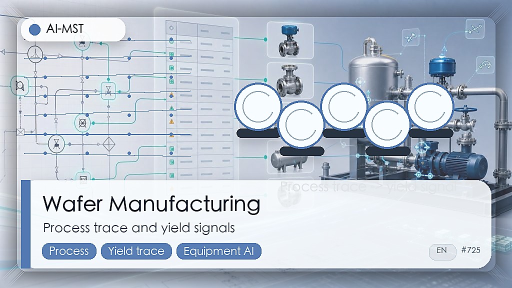
From sand to chip requires 7 core steps and 1000+ process operations over 2-3 months. A single 300mm wafer yields hundreds to thousands of chips. AI has deployment value at every stage, particularly lithography, etch, and CMP.
The chip inside your smartphone started as a handful of sand. Transforming silicon dioxide into a wafer worth tens of thousands of dollars requires over a thousand process steps, hundreds of precision tools, and months of manufacturing time. This is, without exaggeration, the most complex and precise manufacturing process ever devised by humankind.
In this article, we walk through the complete wafer manufacturing journey from start to finish — not just a surface-level overview, but a real understanding of what happens at each stage, why it matters, and how AI is reshaping the entire process.
1. What Exactly Is a Wafer?
A wafer is a thin disc of ultra-pure monocrystalline silicon. It serves as the “canvas” for all integrated circuits — the transistor patterns that make up a chip are etched directly onto this silicon surface.
But making that disc is far more complex than it sounds.
From Quartz Sand to Polysilicon
Everything begins with quartz sand (SiO2). Through an electric arc furnace reduction process, quartz sand becomes metallurgical-grade silicon at roughly 98% purity. But semiconductors demand silicon at 99.999999999% purity (eleven 9s), so additional refinement via the Siemens process or fluidized bed reactor is required to produce electronic-grade polysilicon.
To put that purity in perspective: it is equivalent to an Olympic swimming pool of water containing no more than a single drop of impurities.
Crystal Growth: The Czochralski Method
Polysilicon is melted in a quartz crucible at temperatures above 1,420°C. A small seed crystal is then dipped into the molten silicon and slowly rotated upward. Silicon atoms align along the seed’s crystal lattice, gradually forming a cylindrical monocrystalline silicon ingot.
Today’s standard ingots are 300 mm (12 inches) in diameter and can weigh several hundred kilograms. Growing a single ingot typically takes dozens of hours, with temperature control precision within ±0.5°C. Any fluctuation in pull speed, rotation rate, or thermal gradient can introduce crystal defects.
Slicing, Lapping, and Polishing
Once the ingot is grown, it is sliced into thin wafers (approximately 775 µm thick) using diamond wire saws, then subjected to:
- Lapping: Removes surface damage caused by the wire saw
- Chemical Mechanical Polishing (CMP): Brings surface roughness down to sub-nanometer levels (Ra < 0.5 nm)
- Cleaning: RCA cleaning processes remove surface particles and metallic ion contamination
The result is a mirror-smooth silicon wafer — so flat you can literally see your reflection in it. A single bare wafer at this stage is already worth hundreds to over a thousand dollars. And the truly valuable work has not even begun.
2. The 7 Core Process Steps in Wafer Fabrication
After receiving bare wafers, chip manufacturing enters its core phase — the Front-End-of-Line (FEOL). In simplified terms, fabrication means repeatedly executing these seven fundamental steps for each circuit layer. Advanced-node chips may require over a thousand total process steps.
1. Thermal Oxidation
What it does: Grows a high-quality silicon dioxide (SiO2) film on the wafer surface.
Why it matters: SiO2 is a natural insulator and protective layer, and it forms the gate oxide foundation for MOS transistors. Its quality directly determines transistor electrical performance and reliability.
How it works: Wafers are loaded into high-temperature furnace tubes (900–1,200°C) with oxygen or steam flow. Silicon reacts with oxygen to form a dense oxide layer. Dry oxidation produces higher-quality films but is slower; wet oxidation is faster but yields slightly lower film quality.
Key equipment: Vertical/horizontal oxidation furnaces (Kokusai, TEL, NAURA, etc.).
Where AI helps: Oxide thickness uniformity is highly sensitive to temperature field distribution. AI can build predictive models linking temperature, gas flow, and film thickness, enabling real-time adjustment of furnace zone temperatures to improve within-wafer uniformity from ±2% to below ±0.5%.
2. Photolithography
What it does: Transfers circuit patterns onto the wafer. This is the most critical — and most expensive — step in chip manufacturing.
How it works: A photoresist layer is spin-coated onto the wafer surface. Light passes through a mask (reticle) to project circuit patterns onto the resist. Exposed areas undergo chemical changes; after development, the desired pattern remains.
Key equipment: The lithography scanner is the crown jewel of semiconductor equipment. ASML’s EUV systems (extreme ultraviolet, 13.5 nm wavelength) cost over $300 million each, with global annual production of only a few dozen units. Coat/develop track systems are predominantly supplied by TEL.
Where AI helps: Lithography involves hundreds of parameters — exposure dose, focus offset, overlay accuracy, and more. AI can learn from historical exposure data to predict optimal parameter combinations, reducing test wafer waste. It also accelerates OPC (Optical Proximity Correction) computation, cutting mask design time by several fold.
3. Etching
What it does: Transfers the lithographically defined pattern into the underlying material layer.
How it works: Two main approaches — wet etching (chemical solution, isotropic) and dry etching (plasma bombardment + chemical reaction, anisotropic). Advanced nodes use dry etching almost exclusively because of the need for precise vertical sidewalls.
In 3D NAND and FinFET processes, high-aspect-ratio etching (HAR Etch) is among the toughest challenges. Etch depths reach several micrometers while opening widths are only tens of nanometers — equivalent to drilling a well hundreds of meters deep through the cross-section of a human hair.
Key equipment: Plasma etch systems from Lam Research, TEL, AMEC, and others.
Where AI helps: During etching, plasma state, chamber wall deposits, and gas flows are all changing dynamically. AI monitors plasma conditions in real time via OES (Optical Emission Spectroscopy) and other sensor data, precisely determining etch endpoints and predicting etch rate drift.
4. Ion Implantation
What it does: Implants dopant atoms (e.g., boron, phosphorus, arsenic) into specific wafer regions to modify silicon’s electrical properties.
How it works: Dopant elements are ionized and accelerated to high energies (keV to MeV range), then precisely “shot” into the silicon. Implant depth is controlled by acceleration energy; dose is controlled by beam current and time. Post-implant high-temperature annealing repairs lattice damage and activates the dopants.
Key equipment: Ion implanters from Applied Materials, Axcelis, and others.
Where AI helps: Dose accuracy and uniformity are critical yield indicators. AI can optimize beam stability and wafer scan paths, while intelligently tuning annealing temperature profiles to maximize dopant activation rates.
5. Thin Film Deposition
What it does: Deposits various functional films — insulating layers, conductive layers, barrier layers — onto the wafer surface.
How it works: Two primary methods:
- CVD (Chemical Vapor Deposition): Precursor gases react on the wafer surface to form thin films. Variants include LPCVD, PECVD, and ALD (Atomic Layer Deposition). ALD deposits one atomic layer at a time, achieving angstrom-level thickness control.
- PVD (Physical Vapor Deposition): High-energy particles sputter target material atoms onto the wafer. Primarily used for metal layers.
Key equipment: Systems from Applied Materials, Lam Research, ASM International, NAURA, and others.
Where AI helps: Film thickness, composition, and stress are influenced by dozens of process parameters. AI builds multi-parameter, multi-response predictive models to simultaneously optimize thickness uniformity and step coverage, while using equipment sensor data to predict chamber condition degradation and schedule maintenance proactively.
6. Chemical Mechanical Polishing (CMP)
What it does: Planarizes the wafer surface after each deposition or etch step.
Why it matters: Every process step creates surface topography variations. Without timely planarization, subsequent lithography steps lose depth-of-focus control, causing pattern distortion. Advanced nodes require nanometer-level planarity.
How it works: The wafer is pressed face-down against a rotating polishing pad while a slurry containing nano-abrasive particles and chemical reagents is applied. Chemical corrosion and mechanical abrasion work together to achieve global planarization.
Key equipment: Applied Materials (Reflexion series), EBARA, and others.
Where AI helps: CMP removal rate varies dynamically with pad wear, slurry concentration, and pressure distribution. AI predicts removal rate changes in real time, automatically adjusting pressure zones and endpoint detection to minimize within-wafer non-uniformity.
7. Metrology and Inspection
What it does: Measures critical dimensions (CD), film thickness, overlay accuracy, and detects defects. This is not a post-process check — it is quality control woven throughout the entire fabrication flow.
How it works: Techniques include optical CD measurement (OCD/Scatterometry), e-beam inspection, atomic force microscopy (AFM), X-ray fluorescence (XRF), and more. In advanced fabs, metrology stations can account for 15–20% of total equipment count.
Key equipment: KLA dominates this space with over 50% market share, alongside Onto Innovation, Hitachi High-Tech, and others.
Where AI helps: This is one of the most mature AI application areas in semiconductor manufacturing. Virtual Metrology (VM) uses equipment sensor data and AI models to predict process outcomes for every wafer, turning spot-checks into “100% inspection” without additional metrology time. Automatic Defect Classification (ADC) replaces manual review with deep learning, achieving accuracy rates above 95%.
3. The Equipment Perspective — A Semiconductor Tool’s Lifecycle
The previous section covered the process flow. But from an equipment perspective, semiconductor manufacturing presents an entirely different set of challenges.
Design Phase: From Drawings to Hardware
A semiconductor tool — say, an etch system or CVD chamber — contains thousands of components across vacuum systems, gas delivery, RF power supplies, temperature control, and wafer handling. Equipment design typically starts from a P&ID (Piping and Instrumentation Diagram) that maps out every pipe, valve, sensor, and control logic.
Traditionally, engineers take the P&ID and manually build 3D models in SolidWorks, assembling components one by one. For a complex semiconductor tool, this process can take weeks to months. Inconsistencies in modeling practices and component selection between engineers drive up downstream manufacturing and maintenance costs.
Commissioning Phase: The Test Wafer “Black Hole”
After a tool is built, it enters the bring-up (commissioning) phase. Every new tool and every new process requires DOE (Design of Experiments) to find the optimal process window.
The problem is that traditional full-factorial DOE burns through wafers at an alarming rate. An experiment with 6 parameters at 3 levels each requires 729 experimental runs. Even fractional factorial or Response Surface Methodology (RSM) approaches still need hundreds of test wafers. At $100–$1,000+ per 300 mm test wafer, commissioning costs can easily reach hundreds of thousands of dollars.
And commissioning speed directly impacts production ramp — in the semiconductor industry, every day of earlier capacity release translates to millions of dollars in revenue.
Production Phase: The Endless Battle Against Process Drift
Once the tool is running in production, challenges persist. Chamber wall deposits accumulate, RF matching networks age, consumables wear — equipment state continuously drifts, causing process output to shift.
Production demands a real-time closed-loop control system:
- VM (Virtual Metrology): Predicts process quality from equipment data without waiting for metrology station results
- R2R (Run-to-Run Control): Automatically adjusts next-batch process parameters based on previous batch results
- FDC (Fault Detection & Classification): Monitors equipment health in real time and alerts at the first sign of deviation
Together, these three capabilities keep equipment delivering stable yield output through 24/7 continuous production.
4. How AI Is Transforming Every Stage of Semiconductor Manufacturing
By now, a pattern should be clear: every step in semiconductor manufacturing is fundamentally a multi-parameter, nonlinear, dynamically changing optimization problem. And that is precisely where AI excels.
In fact, AI’s penetration into semiconductor manufacturing is already far deeper than most people realize.
Design: AI-Driven Automated Modeling
Traditional equipment design relies heavily on senior engineers’ experience. AI is changing this paradigm. Today, AI platforms can take a P&ID as input, learn from a customer’s existing assembly models and standard component libraries, and generate complete 3D assemblies (native SolidWorks .sldasm files). AI-MST’s NeuroBox D platform exemplifies this approach — compressing what traditionally takes weeks of modeling work into hours.
Commissioning: Smart DOE Slashes Test Wafer Consumption
During commissioning, AI’s value is even more direct. Using Bayesian optimization, Gaussian process models, and other algorithms, AI can converge on the optimal process window with a fraction of the experimental runs. After each experiment, the AI model updates its understanding of the parameter space and intelligently selects the next most informative set of conditions.
In practice, this Smart DOE approach (as implemented in AI-MST’s NeuroBox E5200 series) reduces test wafer consumption by up to 80% compared to traditional DOE. This is not just cost savings — it means dramatically shorter qualification timelines for new tools and processes, accelerating time-to-production.
Production: Edge AI Enables Millisecond-Level Closed-Loop Control
In volume production, data volumes explode — a single tool can generate thousands of sensor data points per second. Sending all data to the cloud for processing introduces latency and bandwidth constraints incompatible with real-time control.
Edge AI is therefore the core architecture for production environments. Deploying AI inference directly on the tool or on production-line edge servers enables VM prediction, R2R parameter adjustment, and FDC anomaly detection at millisecond latency. AI-MST’s NeuroBox E3200 series adopts this architecture, integrating VM/R2R/FDC on a single edge AI platform with 50 ms inference — from data collection to control command dispatch, the entire loop completes faster than the blink of an eye.
These are not future aspirations. They are production realities already deployed in an growing number of fabs and equipment companies worldwide.
Final Thoughts
From a grain of sand to a finished chip, this journey spans materials science, quantum physics, precision mechanics, chemical engineering, and control theory — virtually every engineering discipline. AI is making this already astonishingly precise manufacturing system faster, more accurate, and more intelligent.
For semiconductor professionals, understanding the full picture of wafer manufacturing is not just about accumulating knowledge. It is about seeing how your specific domain connects to everything upstream and downstream — how your lithography step feeds into etch, how your tuned parameters get validated by metrology, how your equipment’s condition changes ripple through overall yield.
Semiconductor manufacturing has never been about isolated technologies. It is a tightly coupled system of systems. And AI is becoming the intelligent thread that connects them all.
Related Reading
- The Complete Guide to Semiconductor Equipment: 8 Major Categories Explained
- Semiconductor Process Flow: Every Step from Wafer to Chip
- AI in Semiconductor Manufacturing: Intelligent Upgrades from Design to Production
NeuroBox E3200 VM + R2R: real-time quality prediction and auto compensation on every wafer.
Learn about production AI →这篇属于 NeuroBox D 设计自动化场景
获取一份 NeuroBox D 设计自动化评估,看看 P&ID 到 SolidWorks 原生装配体如何接入您的工程流程。
把 P&ID 图纸类型、客户零件库现状、3D 空间边界和装配规则发给我们。工程团队会先判断适合从哪一个机械设计环节切入,再给出落地建议。
- 适合设备商、气路/机械设计、CAD 自动化和工程复核团队
- 可从 P&ID、SolidWorks 零件库、装配规则和空间边界开始
- 优先评估旁接式本地 D 盒子,不要求上传机密图纸到公有云
Discover how MST deploys AI across semiconductor design, manufacturing, and beyond.