CMP Virtual Metrology: AI-Predicted Thickness and Uniformity Control
Key Takeaway
CMP virtual metrology (VM) predicts post-polish thickness and removal rate in real time without stopping the wafer for physical measurement. AI models trained on pad pressure, slurry flow, rotation speed, and conditioning data achieve MAPE below 5% and sub-50ms latency, enabling closed-loop R2R control that reduces within-wafer non-uniformity (WIWNU) by 30–60%. MST’s NeuroBox E5200S deploys CMP VM with as few as 15 conditioning wafers — 80% fewer than traditional DOE.
Why CMP Is the Process That Needs Virtual Metrology Most
Chemical Mechanical Planarization (CMP) sits at one of the most critical junctures in semiconductor manufacturing. Whether you are polishing STI isolation layers, inter-metal dielectric (IMD), tungsten plugs, or copper interconnects, the thickness and uniformity of the polished surface directly determines yield at every downstream lithography step.
Yet CMP has long been managed reactively. Engineers collect post-polish thickness data using a 4-point or 49-point optical metrology tool, wait for the results, and only then decide whether to adjust the next lot’s process recipe. By the time an out-of-control event is detected, dozens of wafers may already be compromised.
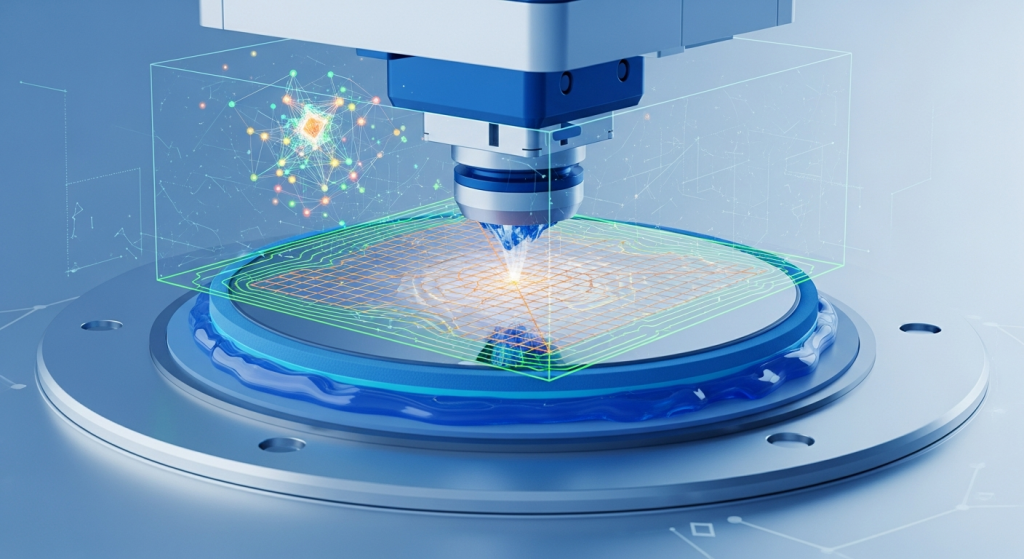
Virtual metrology changes this completely. Instead of measuring after the fact, CMP VM uses the real-time sensor data generated during polishing to predict the final thickness — before the wafer even leaves the polish head.
What CMP Virtual Metrology Actually Predicts
A well-designed CMP VM model predicts three primary outputs:
- Post-polish film thickness — The remaining dielectric or metal layer thickness after CMP, typically in Angstroms or nanometers.
- Material removal rate (MRR) — How fast material is being removed per unit time, used to adjust polish time mid-lot.
- Within-wafer non-uniformity (WIWNU) — Radial and azimuthal thickness variation across the wafer surface, critical for overlay control.
Predicting these three values in real time gives process engineers the ability to close the loop: if the model predicts the current wafer is heading toward under-polish, the system can either extend polish time or flag for review — automatically, without human intervention.
Key Input Features for CMP VM Models
The accuracy of a CMP virtual metrology model depends entirely on which sensor signals you feed it. Based on MST’s deployments across multiple CMP tool platforms (Applied Materials Reflexion, Ebara FREX, Novus), the following features consistently rank as the most predictive:
1. Carrier and Platen Dynamics
- Down force / carrier pressure (zone-by-zone for multi-zone heads)
- Platen and carrier rotation speed (RPM)
- Carrier oscillation position and velocity
- Motor current on both carrier and platen drives
2. Slurry Delivery
- Slurry flow rate (mL/min)
- Slurry temperature at the point of delivery
- DIW back-side rinse flow
3. Pad Condition State
- Pad conditioning disc down force
- Conditioner oscillation sweep speed
- Cumulative pad usage (wafer count since last pad change)
- Acoustic emission signal during conditioning
4. In-Situ Endpoint Detection Signals
- Optical endpoint (OEP) reflectance at 400–900 nm wavelengths
- Eddy current sensor output (for copper and tungsten CMP)
- Motor current change rate (as a proxy for surface transition)
A typical CMP VM feature vector contains 40–80 signals sampled at 10–100 Hz throughout the polish cycle. The model processes these into a thickness prediction within 50 milliseconds of cycle completion — fast enough to feed directly into a run-to-run (R2R) controller for the next wafer.
Model Architecture: Why Hybrid Models Outperform Pure ML
Early CMP VM implementations used simple linear regression on MRR, often called the Preston equation model: MRR = K × P × V, where K is the Preston coefficient, P is down force, and V is relative velocity. This works reasonably well in a stable process window but breaks down the moment the pad starts aging or slurry chemistry drifts.
Modern CMP VM at leading fabs uses a hybrid approach:
- Physical model layer — A simplified Preston-based model captures the fundamental mechanics. This layer ensures physical plausibility even when the ML model is extrapolating slightly outside the training distribution.
- ML correction layer — A gradient-boosted tree (XGBoost) or shallow neural network learns the residual between the physical model’s prediction and actual measured thickness. This layer captures pad aging, slurry variation, and tool-to-tool differences.
- Uncertainty quantification — A Bayesian wrapper estimates prediction confidence. When the model’s uncertainty exceeds a threshold (typically ±8Å for 28nm node), the system flags the wafer for mandatory physical measurement rather than relying on the VM prediction.
MST’s NeuroBox E5200S implements this architecture out of the box. The physical layer is pre-calibrated for common CMP process families (oxide, tungsten, copper, barrier), while the ML layer adapts to each specific tool’s process signature during the commissioning phase.
CMP Smart DOE: Cutting Commissioning Wafers by 80%
One of the biggest obstacles to deploying CMP VM has traditionally been the data collection phase. To build a reliable model, engineers need training data that spans the full operating space — different down forces, rotation speeds, slurry flows, and pad age states. A traditional full-factorial DOE for a typical CMP process might require 80–150 wafers to cover this space adequately.
At $200–400 per production wafer (for advanced nodes), that’s a $16,000–$60,000 data collection cost before the model is even trained.
MST’s Smart DOE for CMP reduces this to 15–20 wafers using two techniques:
- Space-filling design — Latin Hypercube Sampling generates an experiment design that covers the parameter space uniformly with far fewer runs than full-factorial methods. A 5-factor, 5-level full-factorial would require 3,125 conditions; a 20-point Latin Hypercube covers the same space with equivalent model accuracy.
- Transfer learning from existing data — If the fab already has historical process data (even from non-DOE production runs), NeuroBox E5200S can pre-train the model on historical data and use the DOE wafers purely for fine-tuning. In practice, this reduces the required DOE wafers from 15–20 down to 8–12 for tools with 6+ months of existing process logs.
The result: a CMP VM model is typically production-ready within 2–3 weeks of tool connection, compared to 3–6 months for a traditionally planned VM project.
Closing the Loop: CMP VM + R2R Control
Virtual metrology’s full value is realized when it feeds a run-to-run (R2R) controller. The closed-loop architecture works as follows:
- Wafer N completes CMP. The VM model predicts its post-polish thickness within 50ms.
- The R2R controller compares the VM prediction to the target thickness.
- If the prediction is within spec (±1σ), no recipe change is made.
- If the prediction shows a drift trend (e.g., 3 consecutive wafers trending 5Å below target), the R2R controller automatically adjusts the next wafer’s polish time or down force.
- For out-of-limit predictions, the system can halt the lot and request an offline physical measurement before proceeding.
In a 300mm fab running CMP 24/7, this translates to measurable yield improvements. MST has observed the following outcomes across deployed CMP VM + R2R systems:
- WIWNU reduction: 30–60% vs. manual recipe management
- Lot-to-lot thickness variation (σ): reduced from ~12Å to ~4Å
- Physical metrology sampling rate: reduced from 100% to 20–30% (the remaining sampling is used for model drift monitoring, not process control)
- Scrap rate from CMP excursions: reduced by 40–70% in copper CMP applications
Tool-to-Tool Matching with CMP VM
High-volume fabs running CMP typically operate 4–8 polishers of the same model, but tool-to-tool variation means that a recipe developed on Tool A does not automatically produce the same thickness on Tool B. Chamber matching — equalizing the process behavior across tools — is one of the most labor-intensive tasks in CMP process engineering.
CMP VM simplifies chamber matching significantly. Rather than running dedicated matching wafers across all tools (which can take 2–3 weeks per matching cycle), engineers can use the VM model’s internal feature importances to identify which mechanical parameters are most different between tools. In most cases, the top 2–3 differences (e.g., pad conditioning down force on Tool B is 3% lower than nominal, slurry flow on Tool C has 8% higher variance) explain 90% of the thickness offset.
NeuroBox E5200S includes a built-in chamber matching module that automates this analysis. The system continuously monitors the VM model residuals across all tools and flags when a tool is beginning to drift out of the matched window — allowing preventive maintenance scheduling before the tool causes yield loss.
Deployment Checklist: What You Need Before Installing CMP VM
Before deploying virtual metrology on a CMP tool, verify the following prerequisites:
| Prerequisite | Requirement | Notes |
|---|---|---|
| SECS/GEM connectivity | GEM300 or HSMS-SS required | NeuroBox E5200S supports both standards natively |
| Sensor data logging | EAP trace data at ≥1 Hz sampling | Most modern CMP tools log at 10–100 Hz by default |
| Endpoint detection hardware | OEP or eddy current sensor required for metal CMP | Optional for oxide CMP (time-mode polish) |
| Baseline metrology data | Minimum 50 wafers of paired process + metrology data | Reduces further with transfer learning |
| MES integration | Lot and wafer ID linkage to process data | Required for R2R controller deployment |
CMP VM for Advanced Packaging: A Growing Frontier
While CMP VM has been standard practice at leading logic fabs since the 22nm node, adoption in advanced packaging is accelerating rapidly. CoWoS, SoIC, and hybrid bonding processes all involve CMP steps — planarizing redistribution layers (RDL), thinning bonded wafer stacks, and polishing through-silicon vias (TSV) — where thickness and planarity control directly affect interconnect yield.
The challenge in packaging CMP is that the process window is tighter (±5Å on some bonding surfaces), the substrates are thinner and more fragile, and lot sizes are often smaller — making traditional full-factorial DOE even less practical.
Smart DOE + VM is therefore an even more compelling solution for packaging CMP than for front-end CMP. MST is currently working with two OSAT customers on NeuroBox E5200S deployments specifically targeting hybrid bonding CMP qualification.
Getting Started: The 3-Week CMP VM Deployment Path
MST’s standard CMP VM deployment follows a structured 3-week timeline:
- Week 1 — Connection and data audit: NeuroBox E5200S connects to the CMP tool via SECS/GEM. The system audits 3–6 months of historical EAP trace data and identifies the highest-quality process runs for baseline model training.
- Week 2 — Smart DOE and model training: A 15-wafer Smart DOE is executed to cover the key process variables. The model is trained on the combination of historical data and DOE results. Initial MAPE is benchmarked against physical metrology.
- Week 3 — Validation and R2R activation: The VM model runs in shadow mode (predicting but not controlling) for 3 days to validate against physical measurements. Once MAPE is confirmed below 5%, the R2R controller is activated and physical metrology sampling is reduced to 20–30%.
The total investment — hardware, software, and deployment services — typically achieves payback within 6–9 months through reduced metrology cost, lower scrap rates, and higher throughput from reduced hold times.
If your fab is running CMP and managing thickness control manually or with periodic offline measurements, contact MST to discuss a CMP VM pilot. We typically start with one tool and one process layer — the results speak for themselves.
读完这篇,下一步可以很具体
获取一份产线 AI 评估,看看 NeuroBox E3200 / SECS/GEM 怎么接到您的设备。
把设备类型、当前数据接口、工艺目标或良率问题发给我们。工程团队会先判断适合 VM、R2R、Smart DOE、EIP 还是能源优化,再给出下一步建议。
- 适合晶圆厂、设备商、工艺/设备/自动化团队
- 可从 SECS/GEM、Modbus、PLC、CSV/历史数据开始
- 不需要先提交机密 recipe 或客户图纸
Deploy real-time AI process control with sub-50ms latency.